Microelectronics and nanoelectronics testing

A special area of expertise at Fraunhofer IKTS is the use of microscopy principles in the transmission-based characterization of components and composites for micro- and nanoelectronics. For this, the application scope of X-ray-based methods is extended to approx. 50 nm to enable three-dimensional visualization of complex geometries.
X-ray microscopy and tomography


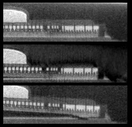
At Fraunhofer IKTS, structures and defects in materials are analyzed by means of X-ray microscopy (XRM) and a method based on it, X-ray nanotomography, performed in an X-ray microscope. These methods enable non-destructive examination of structural and functional materials on a microscopic scale with a resolution of up to approx. 50 nm. Imaging of pores, inclusions, and cracks in composite materials (e.g., CMCs), nanoporous materials (filter membranes), and microelectronics (through-silicon vias) represents the main application. Objects larger than the field of view (max. 65 x 65 μm) can be visualized through sectioning in the X-ray microscope and pasting together of the micrographs to form mosaics.
Especially for low-density materials, the contrast can be enhanced using the Zernike phase contrast technique. This allows for better visualization of interfaces and surfaces as well as delaminated regions and cracks. Thorough materials characterization can be performed at Fraunhofer IKTS through a combination of X-ray microscopy and X-ray nanotomography in conjunction with numerous imaging and analysis methods, such as optical microscopy, micro-CT, electron microscopy (REM, TEM) including spectroscopy (EDX, EELS), and micro- and nanoindentation.
In situ experiments
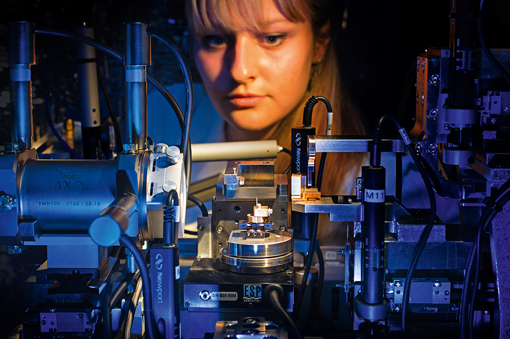
With miniaturized thermal and mechanical testing devices situated in the beam path of the X-ray microscope, both three-dimensional and four-dimensional data can be acquired in experiments. Currently, the following miniaturized testing capabilities are available for use in the X-ray microscope:
- Microindenter with variable test specimens (flat punch, sphere, Berkovich, cube corner) up to 1 N
- Micro double cantilever beam for studying crack propagation
- Microreaction chamber with temperatures of up to 500 °C (reactive or inert atmosphere)
- Electromigration and stress migration test methods