The prerequisites for future microelectronic components that are smaller, more powerful, and simultaneously more reliable are new materials and better technologies. The "Materials and Reliability for Microelectronics" working group at Fraunhofer IKTS is a world leader in the field of micro- and nanomechanical materials characterization and in complex reliability analysis of semiconductor, consumer, and automotive electronics.
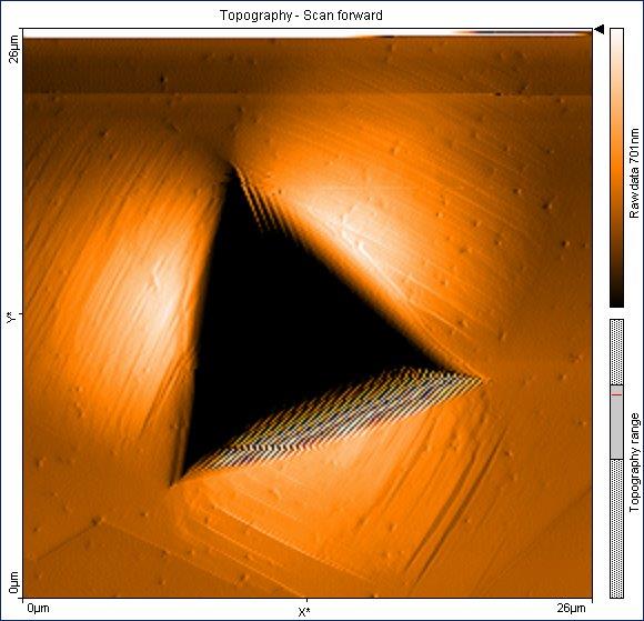
The group's work is based on an in-depth understanding of materials and manufacturing technologies. Using suitable characterization methods, physical degradation mechanisms (stress migration, electromigration, time-dependent dielectric breakdown) are elucidated in a temporally and spatially resolved manner. The determined characteristics serve as a basis for modeling and simulation and flow directly into a multiscale materials database for various materials classes on the micrometer and nanometer scales. State-of-the-art equipment for micro- and nanoindentation, in-situ indentation (SEM, TEM) adhesion measurement, four-point bending tests, and double cantilever beam tests are available at Fraunhofer IKTS. In consideration of the design process for complex electronic systems, limiting factors are characterized and described on the nanoscale and employed in optimization of reliability and service life.
Fraunhofer IKTS cooperates with the Dresden Fraunhofer Cluster for Nanoanalysis (DFCNA) and the Dresden Center for Nanoanalysis (DCN) at the Dresden University of Technology (TU Dresden) to offer an unsurpassed abundance of technical infrastructure, methodological knowledge, and experience. Besides collaborating with leading manufacturers in the semiconductor industry, the working group also contributes its nanoscale expertise to generate improved macroscale products in national and international projects conducted with partner research institutions around the world.
