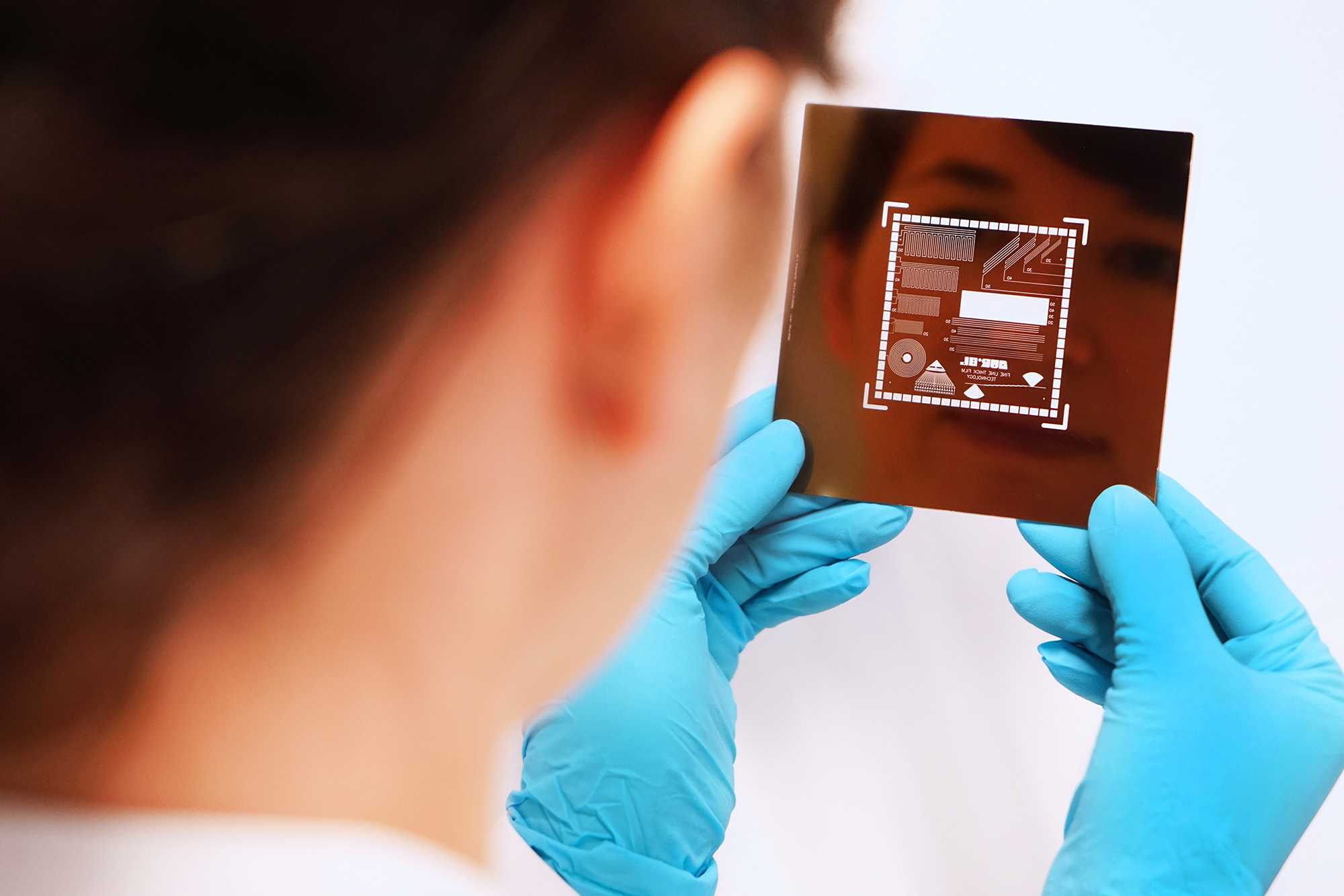
Productronica 2019: Fraunhofer and partners present extremely fine-resolution circuit-board conductors
Photostructurable pastes for 5G applications
For many years now, miniaturization has been the main driver of the electronics industry. This is particularly true for ceramic-based circuit boards, which have properties that make them especially suitable for high-frequency circuits. Increasingly demanding technical requirements have exposed the limits of the classic thick-film technologies used for the production of circuit-board conduc-tors. Now, however, a new generation of thick-film pastes and their photolitho-graphic structuring enable the manufacturing of extremely high-resolution thick-film structures necessary for 5G applications. Moreover, this process is suitable for mass production and industrial applications while maintaining low investment costs and only minimally extending production times. Researchers from the Fraunhofer Institute for Ceramic Technologies and Systems IKTS exhibit the new pastes at the Productronica trade fair in Munich from November 12 to 15 (Hall B2, Booth 228).


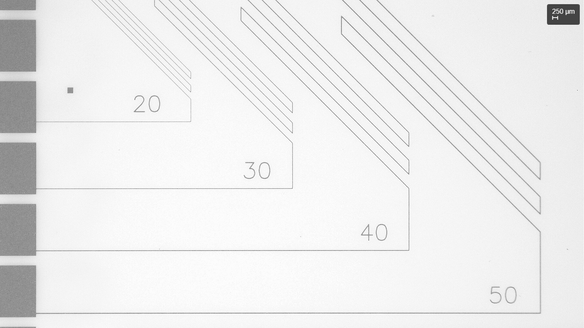
The next generation of mobile internet and mobile telephony is about to arrive: the fifth generation – or 5G, for short. South Korea, Switzerland and a number of U.S. cities are already using 5G. In Germany, the licenses for this standard were auctioned in June 2019. The new technology also means that the electronics used for transmitting and receiving signals will have to be much more finely structured than is currently the case. This applies equally to antennas, which will initially operate at a frequency of 3.6 GHz, before moving to higher frequencies. In terms of miniaturization, the thick-film technology currently used to produce this circuitry has now reached its limits. As far as industrial applications are concerned, a resolution of around 50 micrometers is the absolute limit for this method. In plain terms, this means that the single electrical structures, such as conductors, are minimum 50 micrometers wide. The 5G standard, however, requires circuitry as fine as 20 micrometers and less.
Structures with a resolution no thicker than 20 micrometers
Researchers from the Fraunhofer Institute for Ceramic Technologies and Systems IKTS in Dresden, in cooperation with the UK-based company MOZAIK, have now been able to solve this problem. A corresponding license agreement was signed in June 2019. “We can produce conductors with a resolution of 20 micrometers or less,” explains Dr. Kathrin Reinhardt, research associate at Fraunhofer IKTS. “The process is suitable for mass production and industrial applications, and the investment costs are low.” The process is based on screen-printing technology, the standard industry method, so companies will be able to continue using their current equipment. Screen printing works as follows: a screen with the desired printing pattern is placed on a substrate, and a thick-film paste is pressed through the openings in the screen, thereby applying the pattern to the substrate. In the next step, the layer on the substrate is dried and then sintered at high temperatures, which creates the functional characteristics. However, the stainless-steel wires used to create the screen cannot be produced any thinner than to a certain minimal thickness. So screen printing can only be used to create structures with a minimum resolution of 50 micrometers.
Photoimaging pastes – an additional 15–30 seconds at the most
So-called photoimaging (PI) technology adds two extra steps to the standard process. “Once the thick-film structures have dried on the substrate, we then position a photomask with the final structure above the substrate,” Reinhardt explains. The entire substrate is then illuminated with UV light. A pattern of openings in the photomask allows UV light to pass through to the thick-film layer on the substrate, where it cures a polymers contained in the paste. Those parts of the substrate below the areas of the photomask without any openings are untouched by UV light, meaning that the polymers there remain uncured. The additional step involves a wet chemical development process using water. This step removes those parts of the layer in which the polymers are uncured – i.e., those areas that were covered by the photomask – leaving all the other parts attached to the substrate. Therefore, the previously 50 micrometer wide structures can be reduced to the desired 20 micrometers by this process, the final structure being determined by the photomask. The process now rejoins the normal procedure, whereby the substrate is sintered. Although all this sounds quite elaborate, the whole process is very simple. “In all, the two steps take only between 15 and 30 seconds each,” says Reinhardt. “And they can be easily integrated in the production process.”
PI pastes already available for users
PI technology involves the use of customized thick-film pastes that cure reliably when exposed to UV light but remain unaffected by daylight. In other words, a costly yellow room is not required. The PI know-how comprises the precise tuning of the paste composition. For example, metallizing pastes are made up of metals in powder form (silver, gold or alloys), which will form the structures, along with a UV-cured polymer and various other additives. If there is too much metal in the paste, the layer exposed to UV light will be insufficiently cured, with the result that it will get washed off the substrate during the development process. If, on the contrary, there is too much polymer, the metal structures become porous and can no longer fulfill their function. “We had to take into account two additional parameters while developing the pastes: not just functionality but also the steps of illumination and development,” says Reinhardt. IKTS researchers have already achieved this with pastes containing silver or gold. Now they are working on platinum and resistor pastes. This research is to be unveiled for the first time at the Productronica trade fair in Munich from November 12–15 (Hall B2, Booth 228).
The Italian company Aurel is developing suitable production plants exactly tailored to the new PI pastes from Fraunhofer IKTS. These will also be on show at Productronica (Hall A2, Booth 481). “This extremely promising technology is easily integrated in standard thick-film processes – a field in which Aurel has over 50 years of experience,” explains Fabio Pagnotta, sales and marketing manager at Aurel. “We have therefore opted to launch a high-performance unit, featuring LED illumination and spray jet systems, for use in both small-scale and mass production. The Aurel systems can be used as a standalone unit or as a module incorporated in a fully automated production line, where it will keep pace with the typical cycle times of a standard thick-film production line. Fine lines and combined structures represent a cost-effective alternative to thin-film and solid-state designs for applications such as HF and microwave modules, sensors, chip components, 3D stack interposers and fan-out substrates.”