Fraunhofer Institute for Ceramic Technologies and Systems IKTS
Author / video: Fanny Pohontsch and Andrea Gaal
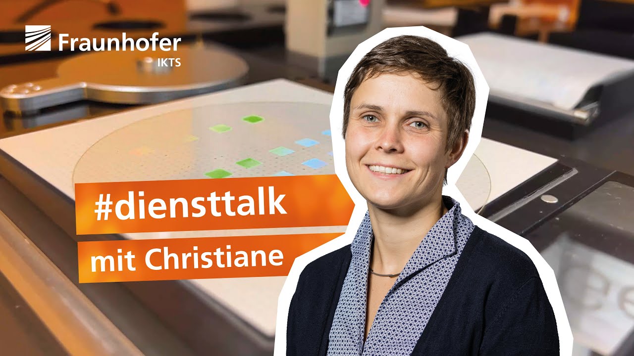
#diensttalk with Dr.-Ing. Christiane Schuster about fine mechanics and nanoscale manufacturing
Our Tuesday feature: In the #diensttalk, our employees give a little insight into their work and reveal the vision that drives them.
Christiane Schuster works on optical testing methods and nanosensor technology at the IKTS site in Dresden-Klotzsche. As head of the working group of the same name, she explains what lies behind this and reveals her personal research highlights to date. We also find out what she is most passionate about.

Christiane, what is the core of your work at the institute?
The core of my work concerns microsystems, specifically those in which mechanical, electrical, fluidic and biochemical properties are integrated alongside optical ones. I was already fascinated by this interaction during my mechatronics studies at Chemnitz University of Technology.
What can we imagine by this specifically? Do you have an application example?
In particular, it's about new types of sensors for optical measurement technology. Together with our partners from a wide range of industries, we develop measuring devices that can be integrated into their production processes. I can give you two examples in particular: Marking solutions for metallic and ceramic components that have to withstand extreme process temperatures of 900 to 1300 °C, and online sensor technology for detecting trace substances in process water. The process water can come from sewage treatment plants, for example, or greenhouses and aquacultures, where the water is sometimes reused several times and recirculated.
In the first area, component marking, we develop inks together with colleagues from other specialist areas that deal with functional materials and materials for printed systems, and industrial partners. These inks are used to print a marking, e.g. a data matrix code, on components. This marking has special optical properties so that it is still legible after the components have undergone forming or harsh production conditions, such as extremely high process temperatures. In this way, the components can be clearly identified, for example in metal processing, and the production process can be monitored right from the start.
Our expertise and our range of services are based on a test stand with which we can test such special inks quickly and close to the industry. When we receive new inks from our customers, we print and read codes and analyze the shape and distribution of the print dots, for example, by using classic image evaluation and machine learning algorithms. The special feature of our test stand is the four integrated cameras, which we can use to evaluate how the inks behave, how stable the print heads are over long periods of time and what proactive service or predictive maintenance can look like. It was particularly exciting to accompany the spin-off of this technology into the start-up Senodis GmbH.
»No matter where the sensor is used, its production and development make my mechatronics heart beat faster.«
And the online sensor technology?
With our online water sensor technology, we can detect small quantities of pharmaceuticals, pesticides or other chemicals directly on site in less than 30 minutes. This means that water samples do not have to be transported to a laboratory first. Results are available almost in real time and can be used to control water treatment. Against the background of protecting water resources, local water treatment is playing an increasingly important role so that water can be reused on site or environmental pollution can be reduced. This is where our sensor comes into play, which is currently being further developed for many exciting, very different applications. I can mention our test container, in which we have demonstrated measurement and treatment technology as part of the fourth purification stage in a sewage treatment plant using the example of the trace substance Diclofenac. Or aquaculture, where the sensor is used to monitor the removal of pollock lice agents from water baths on board of so-called wellboats. I was very impressed to see such a ship as a place of use for our development.
There are many different areas of application that you are working on.
Yes, and no matter where the sensor is used, its production and development make my mechatronics heart beat faster and interdisciplinary cooperation is required. The core element of the sensor is an array of nanopillars that is stamped and coated with gold – precision mechanics and microfabrication at its best. So-called capture structures are then chemically bonded to the gold surface, which in turn capture the analyte molecules from the water samples to be detected later and thus make the sensor specific. Finally, we look at how the sensor works in the laboratory.
But the best thing is to be able to explain to my children or young researchers what we are doing here and what we are doing it for, e.g. as part of their vocational training as a physics laboratory technicians, their BA studies, their final thesis or a volunteer job, and thus get them excited about technology but also about the careful and thoughtful use of resources on our planet.