3D profilometry and digital microscopy for analyzing electronic microsystems

Topic

The high demands placed on electronic assemblies, such as cost reduction, minimization of installation space or high reliability, require reproducible processes. Optical inspection is still an important tool for checking or analyzing errors. It is primarily used to monitor the correct implementation of joining and assembly processes. Our "Reliability of electronic microsystems" working group uses 3D digital microscopy and profilometry for this purpose.
 

3D digital microscopy

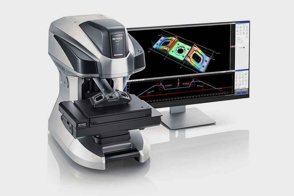
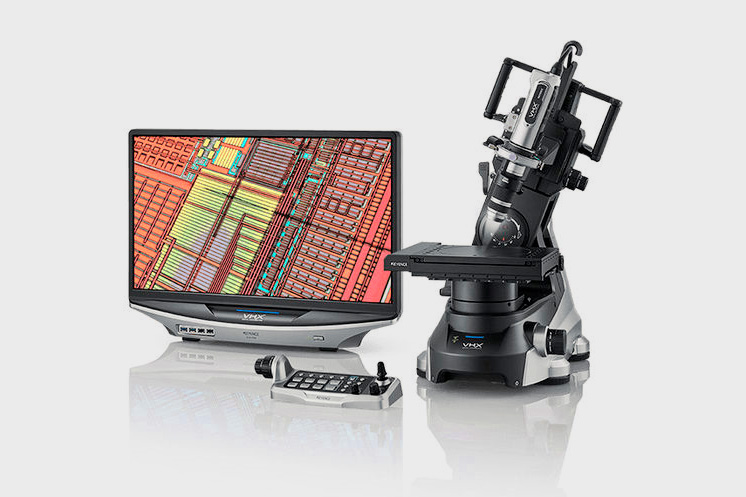
Keyence VHX-5000 digital microscope.
© www.keyence.de
Keyence VHX-5000 digital microscope.
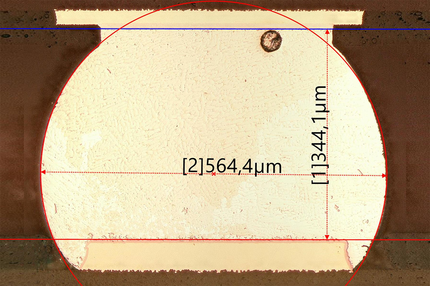
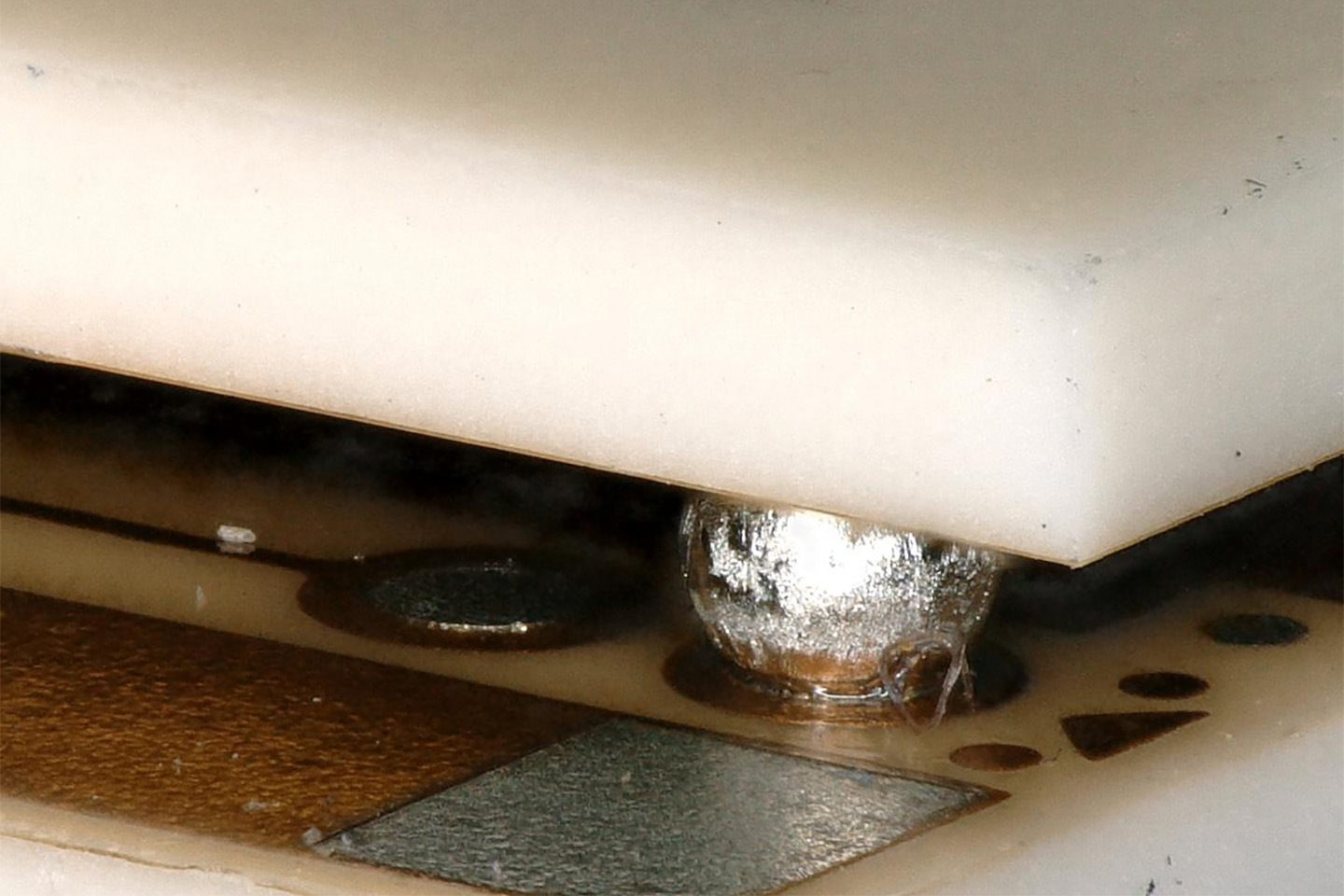
Real solder joint between Al2O3 substrates imaged with high depth of field.
© Fraunhofer IKTS
Real solder joint between Al2O3 substrates imaged with high depth of field.
Measured solder contact on micrograph.
© Fraunhofer IKTS
Measured solder contact on micrograph.
  • Rapid observation of printed circuit boards and microsection samples using an automated xy-table
  • In-house production of metallurgical microsections
  • High depth of field thanks to automatic z-focusing
  • Magnification: 5 to 5000
  • Bright field, dark field, polarizing filter
  • Illumination in incident light, transmitted light, ring light or combined
  • Geometry measurement in 2D and 3D data


3D profilometry

Keyence VR-5200 Profilometer.
© www.keyence.de
Keyence VR-5200 Profilometer.
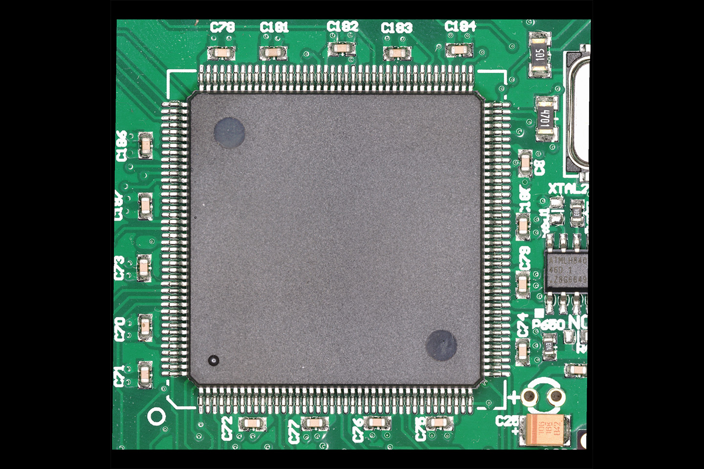
Image of a QFP device.
© Fraunhofer IKTS
Image of a QFP device.
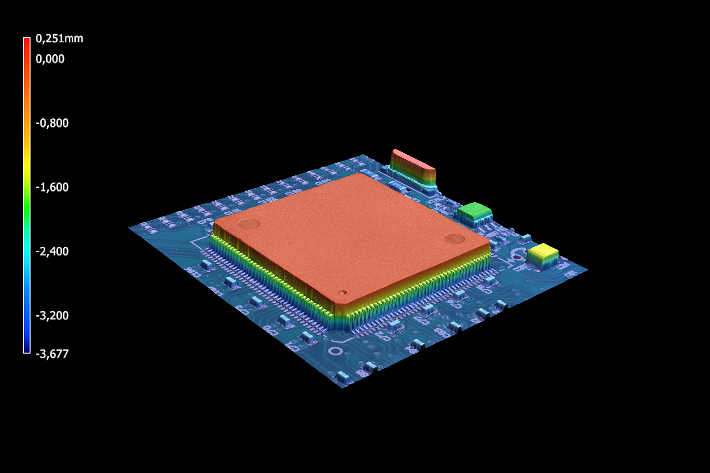
3D rendering of the QFP.
© Fraunhofer IKTS
3D rendering of the QFP.
  • Semi-automated measurement of geometric deviations
  • Measurement of warping of printed circuit boards etc.
  • xy-resolution: 500 nm
  • z-resolution: 100 nm
  • Measuring range: 206 x 104 mm²
  • Measuring accuracy: 2-2.5 µm

Fields of application

Manufacturing-related causes of faults

  • Detection of design errors through routing
  • Errors in the PCB manufacturing process
  • Faulty component assembly and solder paste printing
  • Inadequate quality of supplied components


Aging-related causes of faults

  • Unfavorable material combinations or overloads
  • Cracks in joints (soldering, welding, bonding)
  • Delamination and warping of coating systems

  • Testing the quality of test specimens for in-house characterization
  • Ensuring compliance with specified manufacturing tolerances

NanoFOCUSµScan AF2000 surface measurement system

Application

  • Optical 3D scanning profilometry using various point sensors
  • Measurement of topography, height profile or layer thickness

Characteristics

  • Measuring range: 150 mm x 200 mm
  • Height measuring ranges: 1000 µm–18 mm
  • Height resolution: up to 25 nm
  • Automated measurement sequences


NanoFOCUSµSurf surface measurement system

Application

  • Confocal microscopy using multi-pinhole technology
  • Surface measurement in seconds with high resolution
  • Measurement of topography, height profile or layer thickness

Characteristics

  • Measuring range: up to 50 mm x 50 mm
  • Height measuring ranges: 1 µm–10 mm
  • Height resolution: up to 1 nm


This and other equipment and processes are available to you via the "nanoeva" network.