Optical deformation field measurements

Topic

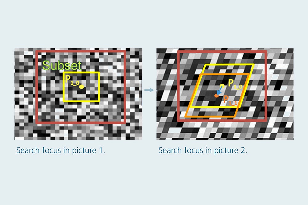
In electronics, thermal fatigue is the most common cause of failure. For a well-founded evaluation of the reliability of a structure, experimental tests are necessary to analyze and determine the physics of failure.

Due to ever shorter product development cycles and the resulting time pressure, supplementary simulations based on finite element models offer a considerable advantage for understanding structural behavior. The scope of experimental tests can thus be considerably reduced. The virtual environment allows both a reliability prediction based on the calculation results and a reliability assessment in a reasonable time.

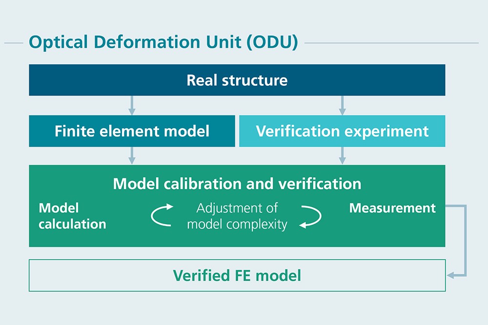
The Optical Deformation Unit (ODU) was developed at Fraunhofer IKTS to confirm the credibility of the results of the FEM calculations. This can be used to carry out deformation experiments that enable FEM model calibration and verification.

© Fraunhofer IKTS
Procedure for calibrating FEM models and verifying optical deformation measurements.

Test-setups for optical measurement (Optical Deformation Unit 1 and 2)

There are few measurement methods that can analyze thermomechanical deformations with high resolution. Digital image correlation makes this possible. It is a powerful tool in conjunction with simulation. The measuring principle is based on the repetition of the following steps:

  1. Registration of features in an evaluation area of the reference state (reference image).
  2. Recognition of these characteristic features in the measurement state (measurement image).
  3. Quantification of the position of the relevant image sections in relation to each other using correlation algorithms.
  4. Determination of the relative displacement of the corresponding points and their surroundings and deformation field visualization.
© Veddac 6 manual (modified)
Illustration according to CWM - Veddac 6 manual.

  • Verification of FEM models through targeted high-resolution measurements on prepared samples.
  • Analysis of the global deformation of entire assembled PCBs or assemblies.
  • Extraction of information on thermal expansion (CTE) and transverse contraction on bulk samples. 


© Fraunhofer IKTS
Optical Deformation Unit 1 (ODU 1, left): effective area 35 x 35 mm², heating up to 180 °C. ODU 2 (right): effective area 140 x 200 mm², heating up to 250 °C.

Example measurement 1: Verification of an FEM model using an embedded CR0805 resistor with ODU 1.
© Fraunhofer IKTS
Example measurement 1: Verification of an FEM model using an embedded CR0805 resistor with ODU 1.

Electronic module during the test in ODU2.
© Fraunhofer IKTS
Electronic module during the test in ODU2.
Temperature profile in the chamber and on the sample.
© Fraunhofer IKTS
Temperature profile in the chamber and on the sample.
Deformation field analysis in the clamping area.
© Fraunhofer IKTS
Deformation field analysis in the clamping area.